
Class 12 Physics में Electronic Devices – इलेक्ट्रॉनिक युक्तियाँ एक महत्वपूर्ण chapter है, जिसमें Semiconductor Electronics के basic concepts और उनके practical applications को सरल भाषा में समझाया गया है। इस chapter में आपको Semiconductor, Energy Bands, Intrinsic और Extrinsic Semiconductor, Doping, n-type और p-type Semiconductor, Electron और Hole जैसे महत्वपूर्ण topics पढ़ने को मिलते हैं। इसके साथ ही p-n Junction, Depletion Region, Potential Barrier, Forward Bias और Reverse Bias को भी आसान उदाहरणों के साथ समझाया गया है।
आगे Semiconductor Diode की I-V Characteristics तथा Rectifier की working को विस्तार से समझाया गया है। इन Class 12 Physics Notes में Hindi और English दोनों भाषाओं में concepts, definitions, important points, formulas और exam-oriented questions दिए गए हैं। ये notes CBSE Board Exam, NCERT आधारित तैयारी और quick revision के लिए उपयोगी हैं। अगर आप Electronic Devices chapter को आसान भाषा में समझना चाहते हैं, तो ये notes आपके लिए एक उपयोगी study resource हैं।
Electronic Devices Class 12 Notes: Diode & Semiconductor
नोट: ये notes NCERT Class 12 Physics के Chapter 14 “Semiconductor Electronics: Materials, Devices and Simple Circuits” की अवधारणाओं को सरल Hindi + English में समझाने के लिए तैयार किए गए हैं। 2026–27 के CBSE syllabus में इस Unit में मुख्यतः energy bands, intrinsic/extrinsic semiconductors, p-n junction, diode की forward/reverse characteristics और rectifier शामिल हैं। (CBSE Academic)
इलेक्ट्रॉनिक युक्तियाँ क्या हैं? | What are Electronic Devices?
Electronic devices वे युक्तियाँ हैं जिनमें electric current और charge carriers के नियंत्रित प्रवाह का उपयोग करके किसी विशेष कार्य को किया जाता है। Semiconductor materials जैसे Silicon (Si) और Germanium (Ge) electronic devices के निर्माण में बहुत महत्वपूर्ण हैं। Diode जैसे semiconductor devices current को नियंत्रित करते हैं और rectifier circuit में AC को DC में बदलने में सहायता करते हैं। आधुनिक computer, mobile, calculator और अन्य electronic systems की मूलभूत समझ semiconductor physics से आती है।
मुख्य बातें:
- Electronic device में current का नियंत्रण किया जाता है।
- Semiconductor इसका प्रमुख material है।
- Silicon सबसे अधिक उपयोग किया जाने वाला semiconductor है।
- Diode एक प्रमुख semiconductor device है।
- p-n junction diode current को मुख्यतः एक दिशा में प्रवाहित करता है।
Semiconductor क्या है? | अर्धचालक
Semiconductor ऐसा पदार्थ है जिसकी electrical conductivity conductor और insulator के बीच होती है। इसकी conductivity temperature और impurities की मात्रा से काफी प्रभावित होती है। सामान्य temperature पर semiconductor में कुछ charge carriers उपलब्ध होते हैं, इसलिए यह थोड़ी conductivity दिखाता है। Temperature बढ़ाने पर अधिक electrons मुक्त होते हैं और conductivity बढ़ जाती है। Silicon और Germanium इसके प्रमुख उदाहरण हैं।
उदाहरण:
- Silicon (Si)
- Germanium (Ge)
विशेषता:
अर्थात semiconductor में temperature बढ़ने पर conductivity बढ़ती है और resistivity घटती है।
Conductor, Semiconductor और Insulator
पदार्थों को उनकी electrical conductivity तथा energy-band structure के आधार पर मुख्यतः conductor, semiconductor और insulator में बाँटा जाता है। इनके बीच मुख्य अंतर valence band और conduction band के बीच energy gap का होता है। Conductor में electrons आसानी से conduction band में उपलब्ध रहते हैं, semiconductor में छोटा energy gap होता है, जबकि insulator में बहुत बड़ा energy gap होता है।
| पदार्थ | Conductivity | Energy Gap | उदाहरण |
|---|---|---|---|
| Conductor | बहुत अधिक | लगभग शून्य | Copper, Aluminium |
| Semiconductor | मध्यम | छोटा | Si, Ge |
| Insulator | बहुत कम | बड़ा | Glass, Rubber |
Energy Bands in Solids | ठोसों में ऊर्जा बैंड
एक isolated atom में electrons निश्चित energy levels में रहते हैं। जब बहुत सारे atoms मिलकर solid बनाते हैं, तो उनके energy levels एक-दूसरे के बहुत पास आकर कई closely spaced energy levels बनाते हैं। इन levels के समूह को energy band कहते हैं। Semiconductor की electrical properties को समझने के लिए मुख्यतः valence band, conduction band और forbidden energy gap का अध्ययन किया जाता है।
मुख्य Energy Bands:
- Valence Band
- Conduction Band
- Forbidden Energy Gap
Valence Band | संयोजकता बैंड
Valence band वह energy band है जिसमें सामान्य अवस्था में valence electrons उपस्थित होते हैं। ये electrons atom के outermost shell से संबंधित होते हैं। सामान्य temperature पर semiconductor के बहुत से electrons valence band में रहते हैं। यदि इन electrons को पर्याप्त energy मिल जाए, तो वे valence band से conduction band में जा सकते हैं। इस प्रक्रिया के बाद valence band में खाली स्थान बनता है जिसे hole कहते हैं।
याद रखें:
- Valence band में bound electrons होते हैं।
- ये electrons सामान्यतः conduction में कम योगदान देते हैं।
- Energy मिलने पर electrons conduction band में जा सकते हैं।
Conduction Band | चालन बैंड
Conduction band वह energy band है जिसमें उपस्थित electrons relatively free होकर electric current के conduction में भाग ले सकते हैं। जब semiconductor के electron को पर्याप्त energy मिलती है, वह valence band छोड़कर conduction band में चला जाता है। इससे electron mobile charge carrier बन जाता है। Semiconductor की electrical conductivity मुख्यतः conduction-band electrons तथा holes के कारण होती है।
मुख्य बिंदु:
- Conduction band में electrons comparatively free होते हैं।
- ये electric current में योगदान देते हैं।
- Temperature बढ़ाने पर conduction electrons की संख्या बढ़ती है।
Forbidden Energy Gap | निषिद्ध ऊर्जा अंतराल
Valence band और conduction band के बीच का वह energy region जिसमें electron के लिए allowed energy state नहीं होती, forbidden energy gap कहलाता है।
इसे से दर्शाते हैं।
जहाँ:
- = conduction band की lower energy
- = valence band की upper energy
- = energy gap
Energy gap जितना कम होगा, electron के लिए conduction band में जाना उतना आसान होगा।
Energy Band के आधार पर पदार्थों का वर्गीकरण
Energy-band theory से conductor, semiconductor और insulator का अंतर आसानी से समझा जा सकता है। Conductor में valence और conduction bands overlap कर सकते हैं, इसलिए electrons आसानी से move करते हैं। Semiconductor में दोनों bands के बीच छोटा forbidden gap होता है। Insulator में यह gap बहुत बड़ा होता है, इसलिए सामान्य परिस्थितियों में electrons conduction band तक नहीं पहुँच पाते।
Conductor
- Valence और conduction bands overlap कर सकते हैं।
- Conductivity बहुत अधिक।
Semiconductor
- छोटा।
- Limited electrons conduction band में जा सकते हैं।
- Temperature बढ़ने पर conductivity बढ़ती है।
Insulator
- बहुत बड़ा।
- Electrons के लिए conduction band में जाना कठिन।
- Conductivity बहुत कम।
Intrinsic Semiconductor | शुद्ध अर्धचालक
ऐसा semiconductor जो chemically pure हो और जिसमें intentionally कोई impurity न मिलाई गई हो, intrinsic semiconductor कहलाता है। Pure silicon और pure germanium intrinsic semiconductor के उदाहरण हैं। Room temperature पर thermal energy के कारण कुछ covalent bonds टूटते हैं और electron-hole pairs बनते हैं। Intrinsic semiconductor में electrons और holes की संख्या बराबर होती है।
जहाँ electron concentration और hole concentration है।
मुख्य बातें:
- यह pure semiconductor होता है।
- इसमें impurity intentionally नहीं मिलाई जाती।
- Electron और hole दोनों charge carriers होते हैं।
- दोनों की संख्या समान होती है।
Covalent Bond in Silicon | Silicon में सहसंयोजक बंध
Silicon के outermost shell में चार valence electrons होते हैं। प्रत्येक Silicon atom अपने आसपास के atoms के साथ electrons share करके covalent bonds बनाता है। इस प्रकार crystal lattice बनता है। सामान्य temperature पर कुछ bonds thermal energy के कारण टूट सकते हैं। Bond टूटने पर एक free electron और एक hole बनता है। यही electron और hole semiconductor में electric conduction में योगदान देते हैं।
याद रखें:
Hole | होल
जब covalent bond से कोई electron निकल जाता है, तो उसके स्थान पर एक खाली स्थान रह जाता है। इस खाली स्थान को hole कहा जाता है। Hole को positive charge carrier माना जाता है। वास्तव में hole कोई अलग physical particle नहीं है; यह electron की अनुपस्थिति को represent करता है। जब पास का electron hole को भरता है, तो hole की स्थिति बदलती हुई दिखाई देती है।
मुख्य बिंदु:
- Hole का effective charge माना जाता है।
- यह positive charge carrier की तरह behave करता है।
- Hole semiconductor में current conduction में योगदान देता है।
Extrinsic Semiconductor | अशुद्ध/डोप्ड अर्धचालक
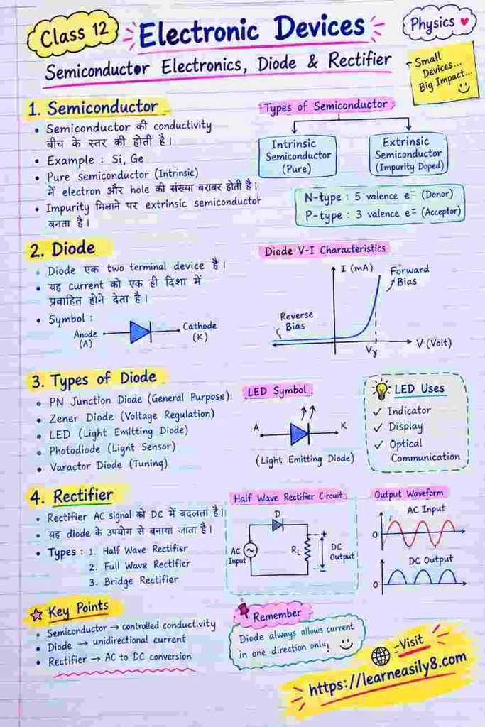
Pure semiconductor की conductivity बढ़ाने के लिए उसमें controlled मात्रा में suitable impurity मिलाई जाती है। इस process को doping कहते हैं और प्राप्त semiconductor को extrinsic semiconductor कहा जाता है। Doping से charge carriers की संख्या बहुत बढ़ जाती है, इसलिए semiconductor की conductivity बढ़ती है। Extrinsic semiconductor मुख्यतः दो प्रकार के होते हैं:
- n-type semiconductor
- p-type semiconductor
Doping | अशुद्धि मिलाने की प्रक्रिया
Intrinsic semiconductor में बहुत कम free charge carriers होते हैं। इसकी conductivity बढ़ाने के लिए बहुत छोटी मात्रा में suitable impurity atoms मिलाए जाते हैं। इस प्रक्रिया को doping कहते हैं। Silicon या Germanium में सामान्यतः Group 13 या Group 15 के elements की impurity मिलाई जाती है। Doping carefully controlled process है क्योंकि impurity की मात्रा बदलने से semiconductor के electrical properties बदल जाते हैं।
Doping के परिणाम:
- Conductivity बढ़ती है।
- Charge carriers की संख्या बढ़ती है।
- Semiconductor को n-type या p-type बनाया जा सकता है।
n-type Semiconductor | n-प्रकार अर्धचालक
जब pure Silicon या Germanium में pentavalent impurity अर्थात पाँच valence electrons वाला atom मिलाया जाता है, तो n-type semiconductor बनता है। Phosphorus, Arsenic और Antimony इसके उदाहरण हैं। Impurity के चार electrons covalent bonds बनाते हैं और पाँचवाँ electron relatively loosely bound रहता है तथा conduction में आसानी से भाग ले सकता है।
इसलिए:
- Majority carriers → Electrons
- Minority carriers → Holes
- Dopant → Pentavalent impurity
- इसे donor impurity कहते हैं।
Donor Impurity | दाता अशुद्धि
Pentavalent impurity semiconductor को एक अतिरिक्त electron उपलब्ध कराती है। इसलिए इसे donor impurity कहा जाता है। उदाहरण के लिए phosphorus के पाँच valence electrons में से चार neighboring Silicon atoms के साथ covalent bonds बनाते हैं। पाँचवाँ electron weakly bound रहता है और थोड़ी energy मिलने पर conduction में भाग ले सकता है।
Examples:
- Phosphorus (P)
- Arsenic (As)
- Antimony (Sb)
p-type Semiconductor | p-प्रकार अर्धचालक
जब pure Silicon या Germanium में trivalent impurity अर्थात तीन valence electrons वाला atom मिलाया जाता है, तो p-type semiconductor बनता है। Boron, Aluminium और Gallium इसके उदाहरण हैं। Impurity atom चार covalent bonds में से एक bond के लिए electron की कमी उत्पन्न करता है। इस electron deficiency को hole के रूप में माना जाता है।
इसलिए:
- Majority carriers → Holes
- Minority carriers → Electrons
- Dopant → Trivalent impurity
- इसे acceptor impurity कहते हैं।
Acceptor Impurity | ग्राही अशुद्धि
Trivalent impurity में तीन valence electrons होते हैं। यह neighboring Silicon atoms के साथ तीन covalent bonds बना सकती है, लेकिन चौथे bond के लिए electron की आवश्यकता होती है। इसलिए यह आसपास से electron accept कर सकती है और semiconductor में hole की स्थिति उत्पन्न होती है। इसलिए trivalent impurity को acceptor impurity कहा जाता है।
Examples:
- Boron (B)
- Aluminium (Al)
- Gallium (Ga)
n-type और p-type Semiconductor में अंतर
n-type और p-type दोनों extrinsic semiconductors हैं, लेकिन उनके majority charge carriers अलग होते हैं। n-type में donor impurity extra electrons उपलब्ध कराती है, जबकि p-type में acceptor impurity holes की concentration बढ़ाती है। दोनों में majority और minority carriers उपस्थित रहते हैं। यह अंतर p-n junction के निर्माण और diode के working को समझने के लिए अत्यंत महत्वपूर्ण है।
| n-type | p-type |
|---|---|
| Pentavalent impurity | Trivalent impurity |
| Donor impurity | Acceptor impurity |
| Electrons majority | Holes majority |
| Holes minority | Electrons minority |
| P, As, Sb | B, Al, Ga |
p-n Junction | p-n संधि
जब p-type semiconductor और n-type semiconductor को एक ही crystal में इस प्रकार बनाया जाता है कि उनके बीच interface बने, तो उस interface को p-n junction कहते हैं। p-region में holes अधिक और n-region में electrons अधिक होते हैं। Junction बनते ही electrons और holes concentration difference के कारण diffuse करते हैं। इस diffusion के कारण junction के आसपास एक विशेष region बनता है जिसे depletion region कहते हैं।
Formation of Depletion Region | रिक्तीकरण क्षेत्र
p-n junction बनने पर n-side के electrons junction की ओर diffuse करते हैं और p-side के holes भी junction की ओर diffuse करते हैं। Junction के पास electrons और holes recombine करते हैं। इससे junction के आसपास mobile charge carriers की कमी हो जाती है। इस क्षेत्र को depletion region कहा जाता है। इसमें fixed ionised donor और acceptor ions मौजूद रहते हैं।
महत्वपूर्ण:
Potential Barrier | विभव अवरोध
Depletion region में fixed positive और negative ions के कारण electric field स्थापित हो जाता है। यह electric field further diffusion का विरोध करता है। इस कारण junction पर एक potential difference विकसित होता है जिसे potential barrier कहते हैं। यह barrier majority carriers को junction पार करने से रोकता है। Applied voltage द्वारा इस barrier को कम या बढ़ाया जा सकता है।
मुख्य विचार:
- Depletion region → electric field
- Electric field → potential barrier
- Barrier majority carrier diffusion को रोकता है।
Semiconductor Diode | अर्धचालक डायोड
एक semiconductor diode मूल रूप से p-n junction device है जिसमें दो terminals होते हैं। p-side को anode और n-side को cathode कहा जाता है। Diode का मुख्य गुण यह है कि यह forward direction में current को आसानी से allow करता है, जबकि reverse direction में current को बहुत कम allow करता है।
मुख्य उपयोग:
- Rectification
- Signal processing
- Switching
- Protection circuits
Forward Bias | अग्र अभिनति
जब p-side को battery के positive terminal से और n-side को negative terminal से जोड़ा जाता है, तो diode forward biased कहलाता है। External electric field potential barrier को कम करता है और depletion region की width घटती है। पर्याप्त applied voltage के बाद diode current तेजी से बढ़ने लगता है।
Forward bias:
परिणाम:
- Depletion width decreases
- Barrier decreases
- Forward current increases
Reverse Bias | उत्क्रम अभिनति
जब p-side को battery के negative terminal से और n-side को positive terminal से जोड़ा जाता है, तो diode reverse biased कहलाता है। External electric field potential barrier को बढ़ाता है और depletion region wider हो जाती है। सामान्य reverse voltage पर बहुत छोटा reverse current flow करता है, जिसे reverse saturation current कहा जाता है।
Reverse bias:
Forward और Reverse Bias में अंतर
Diode की electrical behaviour को समझने के लिए forward और reverse bias का अंतर बहुत महत्वपूर्ण है। Forward bias में applied voltage junction barrier को कम करता है, इसलिए current तेजी से बढ़ता है। Reverse bias में barrier और depletion width बढ़ते हैं तथा केवल बहुत छोटा current flow होता है, जब तक breakdown region नहीं आता।
| Forward Bias | Reverse Bias |
|---|---|
| p → + | p → − |
| n → − | n → + |
| Barrier कम | Barrier अधिक |
| Depletion width कम | Depletion width अधिक |
| Current अधिक | Current बहुत कम |
I-V Characteristics of p-n Junction Diode
Diode की current-voltage relationship को I-V characteristic curve द्वारा दिखाया जाता है। Forward bias में शुरुआत में current बहुत कम रहता है। एक निश्चित voltage के बाद current तेजी से बढ़ता है। Reverse bias में छोटा reverse current flow करता है। बहुत अधिक reverse voltage पर breakdown region प्राप्त हो सकता है।
Important terms:
- Forward current
- Reverse current
- Threshold/Cut-in voltage
- Reverse saturation current
- Breakdown voltage
Threshold Voltage | Cut-in Voltage
Forward bias में diode current प्रारंभ में बहुत कम होता है। एक विशेष voltage के बाद current तेजी से बढ़ने लगता है। इस voltage को threshold voltage या cut-in voltage कहा जाता है।
लगभग:
- Silicon diode →
- Germanium diode →
ये approximate values हैं और practical device तथा conditions पर निर्भर कर सकती हैं।
Reverse Saturation Current
Reverse bias में applied voltage बढ़ाने पर एक बहुत छोटा reverse current flow करता है। एक निश्चित range में यह current लगभग constant रहता है। इसे reverse saturation current कहा जाता है।
यह current मुख्यतः minority charge carriers के कारण होता है।
याद रखें:
जहाँ reverse saturation current को दर्शा सकता है।
Breakdown Voltage | भंजन विभव
जब reverse bias voltage को बहुत अधिक बढ़ाया जाता है, तो एक अवस्था में reverse current अचानक बहुत तेजी से बढ़ सकता है। जिस reverse voltage पर यह phenomenon शुरू होता है उसे breakdown voltage कहते हैं। Breakdown region में current को externally नियंत्रित करना आवश्यक होता है, अन्यथा ordinary diode damage हो सकता है।
Diode as a Rectifier | दिष्टकारी के रूप में डायोड
Rectifier वह electronic circuit है जो AC voltage/current को unidirectional या pulsating DC में बदलता है। p-n junction diode की unidirectional conduction property के कारण इसका उपयोग rectifier के रूप में किया जाता है।
मुख्य प्रकार:
- Half-wave rectifier
- Full-wave rectifier
Rectification का मूल principle है:
Half-Wave Rectifier | अर्ध-तरंग दिष्टकारी
Half-wave rectifier में diode AC input की केवल एक half-cycle को load तक पहुँचने देता है और दूसरी half-cycle को block करता है। इसलिए output में केवल positive या negative half cycles मिलती हैं, depending on diode orientation. यह circuit सरल है लेकिन output में अधिक ripple होता है और इसका rectification efficiency full-wave rectifier से कम होती है।
Working:
- Positive half-cycle → diode conducts
- Negative half-cycle → diode blocks
- Output → pulsating DC
Half-Wave Rectifier का Working
मान लें input AC का positive half-cycle diode को forward bias करता है। तब diode conduct करता है और load resistor में current flow होता है। Negative half-cycle में diode reverse biased हो जाता है और current लगभग zero हो जाता है। इस प्रकार output waveform केवल एक half-cycle की pulses से बनी होती है।
Input:
Output: केवल एक half-cycle की pulses।
Full-Wave Rectifier | पूर्ण-तरंग दिष्टकारी
Full-wave rectifier AC input की दोनों half-cycles का उपयोग करके output में current को एक ही direction में प्राप्त करता है। इसलिए output अधिक continuous pulsating DC जैसा होता है। इसकी ripple frequency input frequency की तुलना में अधिक होती है और यह half-wave rectifier की तुलना में अधिक efficient rectification देता है।
मुख्य बातें:
- दोनों half-cycles का उपयोग।
- Output current एक ही direction में।
- Ripple कम।
- Rectification अधिक effective।
Half-Wave और Full-Wave Rectifier में अंतर
दोनों rectifiers AC को pulsating DC में बदलते हैं, लेकिन input waveform के उपयोग में अंतर होता है। Half-wave rectifier केवल एक half-cycle का उपयोग करता है, जबकि full-wave rectifier दोनों half-cycles का उपयोग करता है। इसलिए full-wave rectifier में output अधिक उपयोगी होता है और ripple frequency अधिक होती है।
| Half-Wave | Full-Wave |
|---|---|
| एक half-cycle | दोनों half-cycles |
| Simple circuit | अधिक complex |
| Output कम | Output अधिक |
| Ripple अधिक | Ripple कम |
| Efficiency कम | Efficiency अधिक |
Electronic Devices Class 12 Notes: Rectifier में Filter का उद्देश्य
Rectifier का output pure DC नहीं बल्कि pulsating DC होता है। यदि circuit को comparatively smooth DC चाहिए, तो rectifier output को filter circuit से गुजराया जाता है। Filter unwanted AC variations या ripple को कम करने में सहायता करता है। Basic electronics में capacitor filter का उपयोग pulsating output को smoother DC में बदलने के लिए किया जा सकता है।
Semiconductor की Temperature Dependence
Semiconductor की conductivity temperature बढ़ने पर बढ़ती है। Temperature बढ़ने से अधिक covalent bonds टूटते हैं और अधिक electron-hole pairs बनते हैं। इसलिए charge carriers की संख्या बढ़ती है और resistance घटती है। यही कारण है कि semiconductor का temperature coefficient सामान्य metals के विपरीत होता है।
अर्थात semiconductor का resistance temperature बढ़ने पर सामान्यतः घटता है।
Electron और Hole Current
Semiconductor में current दो प्रकार के charge carriers के कारण हो सकता है:
- Electrons
- Holes
जब electric field लगाया जाता है, conduction electrons electric field की opposite direction में drift करते हैं। Holes effective positive charge carriers की तरह electric field की direction में move करते हैं। इसलिए semiconductor की conductivity में electrons और holes दोनों का योगदान हो सकता है।
Intrinsic semiconductor में:
Majority और Minority Carriers
Extrinsic semiconductor में जिस charge carrier की concentration अधिक होती है उसे majority carrier कहते हैं और जिसकी concentration कम होती है उसे minority carrier कहते हैं।
n-type:
- Majority → electrons
- Minority → holes
p-type:
- Majority → holes
- Minority → electrons
यह concept p-n junction और diode के operation में बहुत महत्वपूर्ण है।
Semiconductor की Conductivity
Semiconductor की conductivity charge carriers की संख्या और उनकी mobility पर निर्भर करती है। Simplified रूप में conductivity को electrons और holes दोनों के योगदान से समझा जा सकता है।
जहाँ:
- = conductivity
- = electronic charge
- = electron concentration
- = hole concentration
- = electron mobility
- = hole mobility
यह formula concept-based questions में उपयोगी है।
Electronic Devices Class 12 Notes | महत्वपूर्ण सूत्र
Electronic Devices chapter में formulas कम हैं, लेकिन conceptual relationships बहुत महत्वपूर्ण हैं।
Energy gap
Conductivity
Resistivity
Intrinsic semiconductor
Semiconductor relation
Diode का Symbol और Terminals
Diode के दो terminals होते हैं:
- Anode (A) → p-side
- Cathode (K) → n-side
Circuit diagram में diode का symbol current direction और terminal identification को समझने में मदद करता है। Forward bias में conventional current diode के anode से cathode की ओर flow कर सकता है। Practical diode को circuit में लगाते समय polarity का ध्यान रखना आवश्यक है।
Electronic Devices के Important Applications
Semiconductor devices आधुनिक electronic technology की foundation हैं। Diodes का उपयोग rectification, switching और protection circuits में किया जाता है। Semiconductor materials की controlled conductivity के कारण छोटे आकार के devices बनाए जा सकते हैं। यही technology आगे चलकर integrated circuits और complex electronic systems के विकास का आधार बनी।
Applications:
- Power supplies
- Rectifiers
- Switching circuits
- Signal processing
- Computers
- Mobile electronics
- Digital systems
परीक्षा के लिए सबसे महत्वपूर्ण Conceptual Points
Board examination में इस chapter से definitions, differences, diagrams, characteristics और reasoning-based questions पूछे जा सकते हैं। विशेष रूप से p-n junction की formation, depletion region, forward/reverse bias तथा rectifier की working को diagram के साथ समझना चाहिए।
Must Learn:
- Intrinsic semiconductor
- Extrinsic semiconductor
- Doping
- n-type और p-type
- Donor और acceptor
- Majority/minority carriers
- p-n junction
- Depletion region
- Potential barrier
- Forward/reverse bias
- I-V characteristics
- Half-wave rectifier
- Full-wave rectifier
One-Minute Revision | Electronic Devices Class 12 Notes
Semiconductor
→ Conductivity conductor और insulator के बीच।
Intrinsic
→ Pure semiconductor।
Doping
→ Impurity मिलाकर conductivity बढ़ाना।
n-type
→ Pentavalent impurity → electrons majority।
p-type
→ Trivalent impurity → holes majority।
p-n Junction
→ p-type + n-type।
Depletion Region
→ Mobile carriers की कमी वाला region।
Forward Bias
→ p → +, n → − → current अधिक।
Reverse Bias
→ p → −, n → + → current बहुत कम।
Rectifier
→ AC को pulsating DC में बदलता है।
Important Differences for Board Exam
Intrinsic vs Extrinsic Semiconductor
| Intrinsic | Extrinsic |
|---|---|
| Pure | Doped |
| No intentional impurity | Controlled impurity present |
| generally | |
| Conductivity relatively low | Conductivity higher |
Donor vs Acceptor
| Donor | Acceptor |
|---|---|
| Pentavalent | Trivalent |
| Electron देता है | Electron accept करता है |
| n-type बनाता है | p-type बनाता है |
| P, As, Sb | B, Al, Ga |
Forward vs Reverse Bias
| Forward | Reverse |
|---|---|
| p connected to + | p connected to − |
| Barrier decreases | Barrier increases |
| Depletion region decreases | Depletion region increases |
| Large current | Small reverse current |
NCERT-Based Important Questions
Q1. Semiconductor क्या है?
उत्तर: ऐसा पदार्थ जिसकी electrical conductivity conductor और insulator के बीच होती है और जिसकी conductivity temperature तथा doping से नियंत्रित की जा सकती है, semiconductor कहलाता है।
Q2. Intrinsic semiconductor क्या है?
उत्तर: शुद्ध semiconductor जिसमें intentionally कोई impurity नहीं मिलाई गई हो, intrinsic semiconductor कहलाता है।
Q3. Doping क्या है?
उत्तर: Pure semiconductor की conductivity बढ़ाने के लिए उसमें controlled मात्रा में suitable impurity मिलाने की प्रक्रिया doping कहलाती है।
Q4. n-type semiconductor में majority carrier कौन है?
उत्तर: Electrons।
Q5. p-type semiconductor में majority carrier कौन है?
उत्तर: Holes।
Q6. Donor impurity क्या है?
उत्तर: Pentavalent impurity जो semiconductor को अतिरिक्त electron प्रदान करती है, donor impurity कहलाती है।
Q7. Acceptor impurity क्या है?
उत्तर: Trivalent impurity जो electron accept करके hole concentration बढ़ाती है, acceptor impurity कहलाती है।
Q8. Depletion region क्या है?
उत्तर: p-n junction के आसपास वह region जहाँ mobile electrons और holes की concentration बहुत कम हो जाती है, depletion region कहलाता है।
Q9. Diode को forward bias कैसे करते हैं?
उत्तर: p-side को positive terminal और n-side को negative terminal से जोड़कर diode को forward bias किया जाता है।
Q10. Rectifier क्या है?
उत्तर: वह circuit जो AC को unidirectional/pulsating DC में बदलता है, rectifier कहलाता है।
Board Exam के लिए याद रखने वाली Chain
इसे एक sequence की तरह याद करें:
Pure Semiconductor
↓
Doping
↓
Extrinsic Semiconductor
↓
n-type / p-type
↓
p-n Junction
↓
Diffusion
↓
Depletion Region
↓
Potential Barrier
↓
Forward/Reverse Bias
↓
Diode I-V Characteristics
↓
Rectifier
↓
Pulsating DC
Electronic Devices Class 12 Notes: Quick Summary
Electronic Devices chapter semiconductor materials की electrical properties और उनके उपयोग को समझाता है। Semiconductor की conductivity conductor और insulator के बीच होती है तथा temperature और doping से बदलती है। Pure semiconductor intrinsic और doped semiconductor extrinsic कहलाता है। Pentavalent impurity से n-type तथा trivalent impurity से p-type semiconductor बनता है। दोनों को मिलाने पर p-n junction बनता है, जिसके आसपास depletion region और potential barrier विकसित होते हैं।
Diode को forward और reverse bias किया जा सकता है। इसकी unidirectional conduction property के कारण इसका उपयोग rectification में किया जाता है। 2026–27 CBSE syllabus में इस chapter का core focus इन्हीं semiconductor, p-n junction, diode characteristics और rectifier concepts पर है। (CBSE Academic)
NCERT/CBSE reference: NCERT की Class XII Physics textbook listing और CBSE के 2026–27 Physics syllabus के अनुसार Chapter 14 Semiconductor Electronics: Materials, Devices and Simple Circuits Unit IX में रखा गया है। (ncert.nic.in)